EN
 Search for
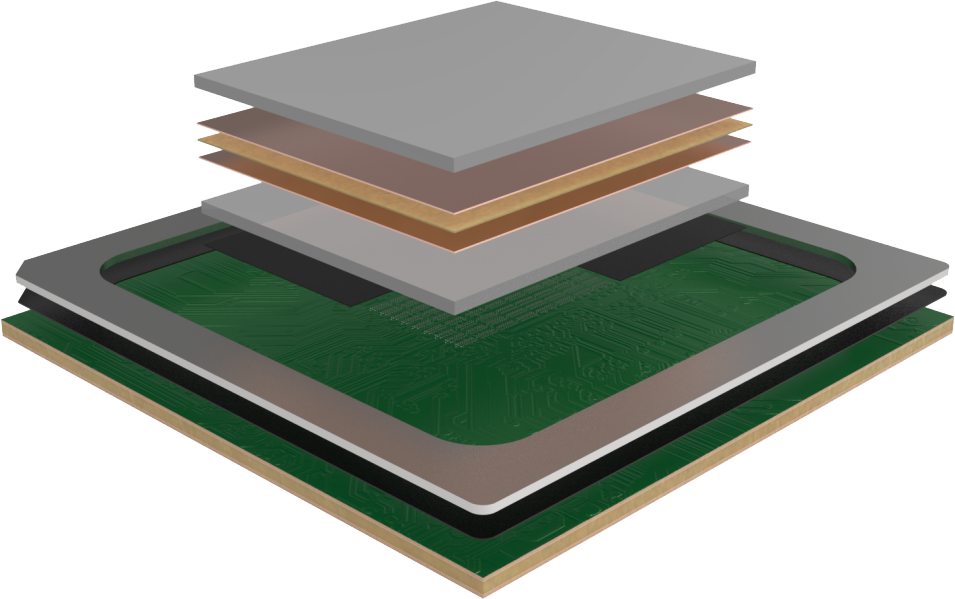
Applying hybrid bonding process, wafers with different fabrication and IPs are bonded together, and then packaged with substrates to achieve integration of storage and computing , and multi IP integration. This packaging asks extremely high requirements for performance like warpage, and heat dissipation.
① Different IP chips through hybrid bondng can reach micrometer spacing , with high rate data transmission and low dissipation, which meets the requirement of high speed, high bandwidth and high power product.
②It can greatly reduce wafer fabrication cost, improve IP repeating utilization rate and shorten products validation cycle by integration of different different fabrication, multiple IPs, and large-sized chips.
